


すべての製品
-
 ブルーノ・ナシメント高品質で手頃な価格の製品を提供してくれてありがとう
 -
 エフサン・サルマリ迅速な回答と専門的な態度により,私たちの協力はより円滑です!
GE DS200VPBLG1AFF VMEバックプレーンボード LCIシリーズ用 多層アーキテクチャ 2kg 重量 1年保証


| 起源の場所 | アメリカ合衆国 |
|---|---|
| ブランド名 | GE |
| 証明 | COO |
| モデル番号 | DS200VPBLG1AFF |
| 最小注文数量 | 1 |
| 価格 | $4000 |
| 受渡し時間 | 5-7日 |
| 支払条件 | T/T |
| 供給の能力 | 999 |
商品の詳細
| 名前 | GE DS200VPBLG1AFF VMEバックプレーンボード | 製品ID | DS200VPBLG1AFF |
|---|---|---|---|
| シリーズ | マークv | 製品ネットの深さ/長さ | 330mm |
| 製品ネット幅 | 100mm | 製品ネットの高さ | 200mm |
| 製品ネットウェイト | 2kg | 保証 | 1年 |
| ハイライト | 多層アーキテクチャ VMEバックプレーンボード,2kg 重量 LCIシリーズバックプレーン,1年保証 GE DS200VPBLG1AFF |
||
製品の説明
GE DS200VPBLG1AFF VMEバックプレーンボード
製品の説明:
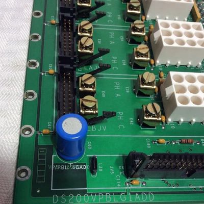
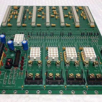
GEのDS200VPBLG1AFF は、Load Commutated Inverter (LCI) シリーズ専用に設計された特殊なVMEバックプレーンボードで、LCI機器のカードケージのJ2およびJ3セクションの中核的な接続ハブとして機能します。その主な役割は、シームレスな信号伝送、安定した電力供給、および重要なLCIコンポーネントのモジュール統合を可能にすることであり、モータードライブやグリッド接続インバーターなどの産業用途におけるLCIシステムの信頼性と効率性を維持するために不可欠です。
特徴的なのは、アナログとデジタルの電源プレーンを物理的に分離した多層アーキテクチャです。この設計により、高感度のアナログ信号と高速デジタル信号間の電磁干渉 (EMI) を最小限に抑え、信号の完全性を維持し、一貫した電力供給を保証します。これは、正確なLCI制御に不可欠です。バックプレーンの各スロットには、バイパスコンデンサと電力供給コンポーネントが装備されており、電圧をさらに安定させ、電力変動によるパフォーマンスの乱れを防ぎます。
J2セクションは、主要なLCIボード向けに調整されており、構造化されたスロットレイアウトを備えています。デジタル信号プロセッサ制御ボード (DSPC) をスロットJ1に、I/OエクステンダーボードをスロットJ3に、ゲート分配およびステータスボード (FCGD) をスロットJ5/J7/J9に、励磁ボードをスロットJ11に、拡張用の2つの予備スロット (J12/J13) をホストします。J1を除くすべてのスロットには、識別を容易にするためにP2コネクタにハードワイヤードスロットIDがあり、デジタルバス信号は信号反射を避けるためにスロットの端で終端します。
J3セクションは、外部接続を管理することにより、スペースの制約に対処します。電流トランス (CT) とその負荷抵抗を統合して電流を監視し、FCGD電圧フィードバック用の電圧スケーリングフィードバックボードへのリンクを有効にし、バックプレーンの電源接続を処理し、柔軟な接地用のスタブコネクタを提供します。これにより、システムの安全性が向上し、EMIが削減されます。
LCI固有のプロトコルとコンポーネントフォームファクタに最適化されたDS200VPBLG1ADDは、LCIハードウェアとのシームレスな互換性を保証し、統合の問題を排除し、要求の厳しい産業環境において、システムが一貫した信頼性の高いパフォーマンスを提供できるようにします。
![]()
推薦されたプロダクト